




For years, India’s semiconductor story was closely associated with chip design and software engineering. The country developed a large pool of engineers working for global semiconductor companies, while domestic efforts increasingly focused on designing chips for specific applications.
SEMICON India 2026 presented a broader picture.
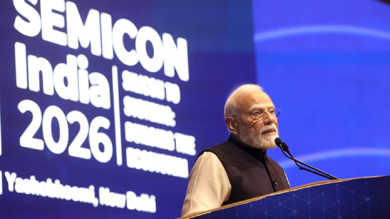
Held from September 17 to 19 at Yashobhoomi in New Delhi, the fifth edition of the event was organised around the theme “Silicon to Systems: Building the Ecosystem.” It brought together industry leaders, policymakers, investors, academics, start-ups and companies working across different parts of the global semiconductor value chain.
The exhibition featured more than 600 exhibitors, including more than 300 international companies, according to a government backgrounder. The event also included a start-up showcase, workforce development pavilion, country and state pavilions and a student hackathon.
The displays demonstrated that the semiconductor ecosystem is much larger than the chip itself. It includes processors, system-on-chips, fabrication, advanced packaging, testing, equipment, materials, software, artificial intelligence, high-performance computing and, importantly, skilled people.
From Silicon to complete computing systems
One of the major themes at the exhibition was the move from individual chip components towards complete computing systems.
The Centre for Development of Advanced Computing (C-DAC) showcased its work in high-performance computing and artificial intelligence, including the AUM HPC-AI Processor and RUDRA-AUM compute node.
The demonstrations reflected an effort to build capabilities at different layers of the computing stack. Instead of limiting semiconductor development to chip design, the ecosystem is increasingly looking at how processors can be integrated into complete computing platforms and systems.
This is particularly relevant as demand for computing grows across artificial intelligence, telecommunications, surveillance, automotive technologies and industrial applications.
The exhibition also showed how Indian start-ups and institutions are working on application-specific processors and chips designed for particular requirements.
Chips designed for everyday technologies
Semiconductors are often associated with smartphones and computers, but the technologies displayed at SEMICON India 2026 showed their much wider role.
Chips are increasingly required in electric vehicles, smart appliances, energy meters, industrial equipment, drones, telecommunications, surveillance systems and connected devices.
Indian chip-design company Vervesemi Microelectronics showcased semiconductor solutions for applications such as motor control, energy meters and data acquisition. These technologies have potential applications in consumer appliances, electric mobility and drones.
Such application-specific chips are important because they demonstrate how semiconductor design can be connected to products and systems used in everyday life.
The development of specialised chips also forms part of India’s effort to build a domestic electronic-system design ecosystem rather than depending entirely on imported semiconductor components.
RISC-V becomes part of India’s indigenous processor push
Another major technology on display was RISC-V, an open instruction-set architecture that can be used to develop processors for different applications.
C-DAC showcased an indigenous 64-bit RISC-V processor, reflecting India’s work in processor design and high-performance computing.
RISC-V is particularly relevant to the domestic semiconductor ecosystem because its open architecture allows developers to design customised processors without relying on a proprietary instruction-set architecture.
Indian companies are also developing their own processor intellectual property around RISC-V.
InCore Semiconductors showcased RISC-V processor IP and system-on-chip design automation technologies. Its processor IP has been silicon-proven across customer chips and technology nodes ranging from 180 nm to 16 nm, according to material associated with the exhibition.
The development of indigenous processor IP is significant because processor architecture and intellectual property form an important part of the semiconductor value chain.
Indigenous broadband technology links processor, software and connectivity
The exhibition also demonstrated how Indian-designed processors can be integrated into communication equipment.
Aheesa Technology showcased an indigenous internet connectivity device capable of speeds of up to 1 Gbps. The system can enable internet service providers to connect approximately 64 homes through a single Optical Line Terminal.
The device uses Vihan, an India-developed software platform, and is powered by C-DAC’s 64-bit RISC-V processor.
This represents a combination of domestic processor technology, software and broadband hardware.
The example illustrates the broader “silicon to systems” approach of SEMICON India 2026: developing a chip is one stage, while integrating it into products that can perform practical functions is another.
AI and semiconductor technology come together
Artificial intelligence was another prominent theme at the exhibition.
As AI applications expand, the demand for specialised hardware capable of processing large amounts of data efficiently is also increasing.
Indian semiconductor start-up Netrasemi showcased AI-capable system-on-chips for applications including secure surveillance, smart sensors, robotics, drones and mobility.
The company has taped out an indigenous AI SoC for CCTV surveillance using a 12 nm process node. The chip integrates AI/ML accelerators along with vision-processing and video-processing engines.
The technology illustrates the growing importance of edge AI, where data can be processed closer to the device rather than always being sent to a central cloud system.
For applications such as surveillance cameras, drones and industrial sensors, local processing can be important for real-time decision-making.
Semiconductor ecosystem extends beyond chips
A semiconductor industry cannot function on chip designers alone.
A complete ecosystem requires fabrication facilities, advanced packaging and testing units, equipment manufacturers, materials suppliers, research laboratories, design companies and trained engineers.
SEMICON India 2026 brought these different components together.
The exhibition included technologies and companies working in areas such as semiconductor materials, manufacturing equipment, testing, packaging and system integration.
The focus on the entire value chain also reflects the direction of India’s semiconductor policy.
The government has increasingly shifted from supporting only individual projects towards building an ecosystem in which companies at different stages of semiconductor production can operate together.
Semicon 2.0 expands India’s semiconductor policy
This wider approach is also reflected in Semicon 2.0, approved by the Union Cabinet in July 2026 with an outlay of Rs 1,27,500 crore.
The programme is built around six strategic pillars: chip design; semiconductor machines and materials; new fabrication facilities; advanced packaging; research and development; and talent development.
The programme builds on Semicon 1.0, which had an outlay of Rs 76,000 crore and focused on creating a domestic semiconductor and display manufacturing ecosystem.
The expanded framework seeks to cover more of the value chain, including the equipment and materials required for semiconductor manufacturing.
This is important because semiconductor manufacturing depends on a complex network of specialised technologies and suppliers.
Policy announcements to semiconductor production
SEMICON India 2026 was held as India’s semiconductor programme entered a phase in which approved projects are moving towards manufacturing and commercial production.
Under the Semicon India Programme, 12 semiconductor projects have been approved across six States, involving committed investment of more than Rs 1.64 lakh crore, according to the latest government information.
The projects cover different areas, including silicon and compound semiconductor fabs, display fabrication and advanced packaging.
Government updates in September said that five facilities had commenced commercial production, reflecting a further movement from project approvals towards operational manufacturing.
This includes facilities associated with companies such as Micron, Kaynes and CG Semi, among others.
The significance of these facilities extends beyond semiconductor manufacturing itself because chips are required across industries including automobiles, telecommunications, aerospace, power electronics and consumer electronics.
Start-ups get a larger role in the ecosystem
Start-ups were another important part of SEMICON India 2026.
The event included a dedicated Start-up Pavilion, providing emerging companies working across semiconductor design, manufacturing, advanced packaging, AI hardware, embedded systems, robotics, electric mobility and deep technology with a platform to display their products and technologies.
The participation of start-ups is important because semiconductor innovation can emerge from smaller companies developing specialised intellectual property and application-specific solutions.
India’s Design Linked Incentive (DLI) Scheme has also supported domestic chip-design projects.
The government has approved projects in areas including surveillance, drones, energy meters, microprocessors, satellite communications, broadband and Internet-of-Things system-on-chips.
More than one lakh engineers get access to chip-design tools
Developing a semiconductor industry also requires a large pool of skilled engineers.
The Chips to Startup (C2S) Programme and the DLI Scheme are being used to expand access to advanced chip-design tools, fabrication services and specialised training.
According to the government, the ChipIN Centre has provided access to more than one lakh engineers from over 500 organisations, including around 400 academic institutions and 100 start-ups.
These organisations have collectively developed more than 300 chip designs for fabrication in India and abroad and recorded more than four crore hours of chip-design tool usage.
The programme is intended to reduce the entry barriers associated with semiconductor design, where access to expensive electronic design automation tools and fabrication facilities can otherwise be difficult for universities and young companies.
Workforce development gets dedicated space
SEMICON India 2026 also included a Workforce Development Pavilion, focusing on the skills required for the expanding semiconductor industry.
The pavilion offered students and faculty exposure to career pathways, industry interactions, research collaborations, internships and employment opportunities.
The emphasis on workforce development reflects a basic requirement of semiconductor manufacturing: infrastructure alone is not sufficient.
Designing chips, operating fabrication facilities, developing packaging technologies and manufacturing semiconductor equipment require specialised engineering and technical skills.
The exhibition therefore connected industry expansion with talent development.
The event also featured a semiconductor DeepTech Hackathon for undergraduate, postgraduate and PhD students.
The programme was designed around real-world semiconductor problems and included mentoring and multiple stages leading to a final presentation at SEMICON India 2026.
The initiative is intended to give students exposure to industry requirements while encouraging them to develop practical solutions.
Such programmes also create a link between universities and semiconductor companies, which is important for building a sustained talent pipeline.
What ‘Silicon to Systems’ means for India
The theme “Silicon to Systems: Building the Ecosystem” captured the larger story visible across the exhibition.
The semiconductor industry begins with materials and manufacturing processes but does not end when a chip comes out of a fabrication plant.
The chip must be packaged, tested and integrated into a product. That product may then become part of a larger system such as a smartphone, vehicle, broadband network, surveillance system, industrial machine or AI platform.
SEMICON India 2026 showcased these different layers together.
The displays ranged from RISC-V processors and AI-enabled SoCs to high-performance computing, broadband equipment, motor-control chips, packaging, materials and manufacturing technologies.
India’s semiconductor story is becoming wider
The most visible change at SEMICON India 2026 was therefore not simply the number of companies participating. It was the breadth of technologies represented.
India’s semiconductor ecosystem is expanding from a primarily design-led base towards a wider structure involving design, fabrication, packaging, testing, materials, equipment, research, AI hardware, start-ups and skilled talent.
The government-backed programmes are supporting this expansion, while private companies and academic institutions are developing products and intellectual property across different parts of the value chain.
The Rs 1.27 lakh crore Semicon 2.0 programme, the approved projects worth more than Rs 1.64 lakh crore, the growing number of commercial facilities and the participation of more than one lakh engineers in shared chip-design infrastructure point to a semiconductor strategy that is increasingly focused on the complete ecosystem rather than one segment alone.
At Yashobhoomi, the central message was therefore broader than chip manufacturing. India’s semiconductor journey is moving from designing individual chips towards building the systems, infrastructure, talent and industrial network needed to turn those designs into products and commercial technologies.