





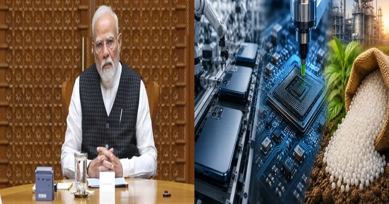
New Delhi: The Union Cabinet on July 15, Wednesday approved seven major decisions, including Semicon 2.0, the Mobile Phone Manufacturing Scheme (MPMS) and the National Investment Policy for Urea-2026, along with infrastructure and railway projects. The total outlay of the approved projects stands at Rs 2,19,353 crore. Addressing the media after the Cabinet meeting, Union Information and Broadcasting Minister Ashwini Vaishnaw said seven major decisions had been taken.
Several landmark decisions taken by the Union Cabinet today, under the leadership of PM @narendramodi. #CabinetDecisions approved:
✅ Semicon 2.0 for development of India's Semiconductor design & manufacturing ecosystem, with a total budget outlay of ₹ 1,27,500 crore.
— Dr. S. Jaishankar (@DrSJaishankar) July 15, 2026
Semicon 2.0
Among the key announcements, the Cabinet approved Semicon 2.0 with an outlay of Rs 1,27,500 crore (USD 13.17 billion) to strengthen India’s semiconductor manufacturing ecosystem. The scheme aims to support chip design, manufacturing, advanced packaging, research, talent development and the production of key equipment and materials needed for the industry.
The programme builds on the progress made under Semicon 1.0 and reflects the government’s long-term commitment to making India a global semiconductor hub.
India’s semiconductor journey gets even more vibrant!
The Cabinet has approved Semicon 2.0 with an outlay of Rs. 1,27,500 crore, reaffirming our long-term commitment to making India a global centre for semiconductor design, manufacturing and innovation. Powered by our youth,…
— Narendra Modi (@narendramodi) July 15, 2026
Semicon 2.0 is based on 6 key pillars:
- Strengthening India’s chip design ecosystem: The government said 105 startups are already developing semiconductor chips. The new scheme will support semiconductor Intellectual Property (IP), chip designs and systems for strategic and commercial use to position India as a leading chip design nation.
- Developing the semiconductor supply chain: Supporting companies involved in the manufacturing and research of semiconductor equipment, materials, chemicals and gases. The government said this will help build a strong domestic ecosystem and improve precision manufacturing.
- Expanding semiconductor manufacturing: This involves encouraging investments in silicon fabs, compound semiconductor fabs, discrete component fabs and display fabs. The government said global confidence in India’s semiconductor strategy has increased, with the country’s first semiconductor fabrication plant expected to be commissioned in 2028.
- Strengthening India’s ATMP line: Focus is on consolidating Assembly, Testing, Marking and Packaging (ATMP) capability and Outsourced Semiconductor Assembly and Test (OSAT) ecosystem by promoting advanced packaging technologies.
- Research and development: To help India move beyond existing semiconductor technology nodes through collaboration with leading research institutions in India and abroad.
- Talent development: The government said 315 universities are using advanced Electronic Design Automation (EDA) tools to train students, with around 68,000 students trained so far. Industry participation will also be expanded to develop specialised skills required for semiconductor manufacturing.
Highlighting the progress made under the India Semiconductor Mission (ISM) 1.0, the government said 12 manufacturing units with cumulative investments exceeding Rs 1.64 lakh crore(USD 17.02 billion) have been approved, including one silicon fab, one silicon carbide fab, one integrated gallium nitride Micro LED display fab and nine packaging units. Commercial production has already begun at Micron, Kaynes and CG Semi, while another unit is expected to commence production later this year.
On the design front, 24 semiconductor design projects have been approved for financial support, while 105 startups and MSMEs have been granted access to industry-standard EDA tools to develop chips for applications such as AI systems, telecom equipment, drones, satellite communications, IoT devices and smart meters.
Vaishnaw also highlighted the growing international confidence in India’s semiconductor ambitions, pointing to strategic partnerships with major semiconductor economies, including the United States (2023 and Pax Silica in 2026), the European Union (2023), Japan (2023), Singapore (2024), the Netherlands (2025) and Germany (2026) as part of efforts to strengthen the country’s semiconductor ecosystem.
India has attracted significant commitments from leading global semiconductor companies. According to information shared by the Minister, Applied Materials and AMD have each announced investments of USD 400 million, while Microchip Technology has committed USD 300 million. Lam Research has announced an investment of USD 1.1 billion and KLA has committed USD 400 million. In addition, ASML, IBL Electron and Merck have signed memoranda of understanding (MoUs) with the Tata Group to support semiconductor ecosystem development in India.
Mobile Phone Manufacturing Scheme(MPMS) & Semicon 2.0 can generate 5 lakh jobs
The Cabinet also approved the Mobile Phone Manufacturing Scheme (MPMS) with an allocation of Rs 62,500 crore. The scheme is one of the major manufacturing-related decisions announced alongside Semicon 2.0.
A massive boost to ‘Make in India’ and our electronics manufacturing ecosystem!
The Cabinet’s approval of the Mobile Phone Manufacturing Scheme, with an outlay of Rs. 62,500 crore will scale up production, deepen domestic value addition, strengthen supply chains and create a…
— Narendra Modi (@narendramodi) July 15, 2026
Meanwhile, the Union Cabinet’s approval of the Semicon 2.0 programme and the Mobile Phone Manufacturing Scheme (MPMS) could generate up to 5 lakh direct jobs and around 15 lakh indirect jobs in the coming years, India Cellular and Electronics Association (ICEA) Chairman Pankaj Mohindroo said.
Speaking on the employment potential of the two schemes, Mohindroo said the benefits would extend across the electronics and semiconductor value chain, from factory-level jobs to high-end chip design and research. He said that the semiconductor sector would also create employment opportunities in highly skilled areas, including semiconductor design and research and development.
“The mobile phone scheme is about scale, sustaining the huge success we’ve had in PLI 1.0 and to go from 15-17 per cent of global manufacturing to over 30 per cent”, Pankaj Mohindroo further said. According to Mohindroo, the semiconductor programme, on the other hand, is aimed at building a strong domestic foundation for chip manufacturing and innovation.
“The objective now is to build a 360 industry with also deep focus on R&D, deep focus on developing our own products, our own designs. The two schemes have a very divergent history, but in the end, they all collide with one objective, which is that to have an end-to-end mobile manufacturing and electronic manufacturing industry”, he said.
He added that India has already built significant scale in mobile phone manufacturing and is now focusing on increasing domestic value addition and strengthening the semiconductor ecosystem. Mohindroo also expressed confidence that the mobile phone manufacturing target announced under MPMS would be surpassed. “So Rs 39 lakh crores production is definitely not impossible. We will not only achieve it, we will cross it”, Mohindroo reiterated.
On exports, he said smartphones have already emerged as India’s largest exported commodity and the industry is aiming for even higher numbers in the coming years. He said that the schemes would help India move towards a competitive and self-reliant electronics manufacturing ecosystem by the end of the decade through greater scale, higher domestic value addition, stronger exports and increased investments in semiconductor technology and innovation.
Global semicon manufacturing is set to hit a record USD 165.9bn in 2026
Global spending on semiconductor manufacturing equipment is set to hit a record USD 165.9 billion in 2026, marking a 23.2 per cent increase over the previous year, according to SEMI’s Mid-Year Total Semiconductor Equipment Forecast. The sustained surge in investments, driven by Artificial Intelligence (AI) and advanced chip technologies, is expected to create significant opportunities for India’s rapidly expanding semiconductor ecosystem.
According to the forecast, global semiconductor equipment spending will continue its upward trajectory to reach USD 229.5 billion by 2028, marking five consecutive years of industry growth. Investments are being fuelled by rising demand for AI-enabled computing, high-bandwidth memory (HBM), advanced logic chips, next-generation packaging technologies and intelligent edge devices.
The report said Wafer Fab Equipment (WFE), the industry’s largest segment, is expected to reach USD 143.9 billion in 2026, while semiconductor test equipment spending is projected to grow 31 per cent to USD 15.3 billion as manufacturers expand production capacity. SEMI President and CEO Ajit Manocha said AI is accelerating demand for more powerful and efficient chips, prompting semiconductor companies to increase investments in leading-edge logic, advanced memory, testing and packaging capabilities.
The global investment cycle comes at a crucial time for India, which has approved 12 semiconductor manufacturing projects across fabrication plants, ATMP/OSAT facilities, compound semiconductors and display manufacturing, representing investments of more than USD 20 billion. Government initiatives, including the Semicon India Programme, Production Linked Incentive (PLI) scheme, Electronics Components Manufacturing Scheme (ECMS), Electronics Manufacturing Clusters (EMC), Research, Development and Innovation (RDI) initiatives and the India AI Mission, are helping build a comprehensive semiconductor ecosystem.
While China, Taiwan and South Korea are expected to remain the world’s largest destinations for semiconductor equipment spending through 2028, regional diversification, government incentives and supply chain resilience efforts are creating fresh opportunities for emerging manufacturing hubs such as India. Rising global demand for semiconductor chips is expected to benefit equipment manufacturers, automation firms, precision engineering companies, speciality material suppliers and component makers looking to expand their presence in the country.
National Investment Policy for Urea
Highlighting another key decision, Minister Vaishnaw said that the government has approved the National Investment Policy for Urea-2026. He said the policy is aimed at making India self-reliant in urea production. The decision is a policy approval and does not carry a financial allocation in the Cabinet decisions table. The policy is considered as critical to ensure India’s agricultural sector and to seek food security amidst volatile geopolitical landscape & distorted supply chains.
देशभर के अपने किसान भाई-बहनों के कल्याण के लिए हमारी सरकार कोई कोर-कसर नहीं छोड़ रही है। इसी कड़ी में आज राष्ट्रीय यूरिया निवेश नीति-2026 के प्रस्ताव को मंजूरी दी गई है। इससे न सिर्फ गैस आधारित नए यूरिया उत्पादन संयंत्रों की स्थापना के लिए निवेश को प्रोत्साहन मिलेगा, बल्कि यूरिया…
— Narendra Modi (@narendramodi) July 15, 2026
Railway projects
Apart from these, the Cabinet also approved two railway infrastructure projects. It cleared the doubling of the Paradeep-Haridaspur railway line at a cost of Rs 2,542 crore. It also approved the fourth railway line between Dangoaposi and Rajkharsawan, involving an investment of Rs 1,365 crore.
A major boost to connectivity and economic growth in Odisha and Jharkhand!
The Cabinet has approved two important railway multitracking projects, the doubling of the Paradeep-Haridaspur line and the fourth line between Rajkharsawan and Dangoaposi. These projects will further…
— Narendra Modi (@narendramodi) July 15, 2026
Infrastructure development in Varanasi
The Minister said that the first two decisions relate to a new approach to infrastructure development in Varanasi (Kashi).
उत्तर प्रदेश में कनेक्टिविटी के विस्तार के साथ वाराणसी में बाबा विश्वनाथ के दर्शन को और अधिक सुगम एवं सुविधाजनक बनाने के लिए हम कृतसंकल्प हैं। इसी दिशा में आज हमारी सरकार ने वरुणा नदी के किनारे 6/4-लेन के एलिवेटेड कॉरिडोर के निर्माण को मंजूरी दी है। यह प्रोजेक्ट न सिर्फ हमारे…
— Narendra Modi (@narendramodi) July 15, 2026
काशी में वर्ल्ड क्लास इंफ्रास्ट्रक्चर के विकास के लिए हम प्रतिबद्ध हैं। इसी कड़ी में आज हमने गंगा के किनारे 6-लेन के अत्याधुनिक कॉरिडोर के निर्माण को मंजूरी दी है। इससे शहर के प्रमुख धार्मिक, शैक्षणिक और सांस्कृतिक स्थलों तक पहुंच और बेहतर होगी। इसके साथ ही रोड नेटवर्क पर यातायात…
— Narendra Modi (@narendramodi) July 15, 2026
According to the minister, the government has approved a 6/4-lane elevated corridor along the River Varuna at a cost of Rs 10,998 crore and a 6-lane elevated corridor along the River Ganga costing Rs 14,448 crore.
(With Inputs from ANI)