





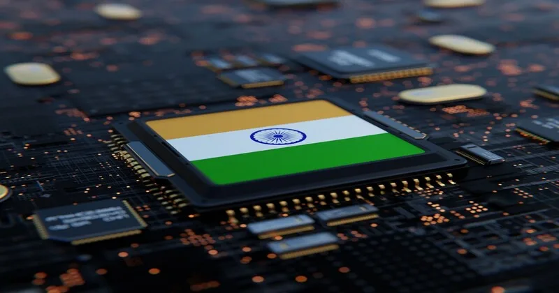
India is building a semiconductor ecosystem that goes beyond chip manufacturing, combining electronics production, chip design, fabrication, packaging, equipment, materials, research and talent development.
With 12 semiconductor units approved and a new Semicon 2.0 phase planned, the government is seeking to turn the country into a major global base for semiconductor design and manufacturing
India is seeking to establish itself as a major global hub for semiconductor manufacturing and chip design, building on the rapid expansion of its electronics manufacturing industry over the past decade.
In an account of the government’s semiconductor strategy, Union Minister for Railways, Information & Broadcasting, and Electronics and Information Technology Ashwini Vaishnaw said the approach is focused on creating a complete semiconductor ecosystem rather than setting up isolated manufacturing facilities.
The strategy covers the entire semiconductor value chain, including chip design, fabrication, packaging, manufacturing equipment, specialised materials, research and development and the development of skilled talent.
The effort has gained importance as semiconductors have become essential to almost every major technology-driven industry. From smartphones and automobiles to aircraft, drones and medical equipment, modern products increasingly depend on sophisticated chips.
For India, the objective is therefore not simply to become another manufacturing location. The larger ambition is to develop capabilities across the semiconductor value chain and create an ecosystem that can support both domestic requirements and global markets.
Why semiconductors have become strategically important
Semiconductors form the foundation of the modern electronics industry. Chips produced by semiconductor companies power an enormous range of devices and systems, making the sector critical to industries far beyond electronics.
The global electronics industry is estimated at $4.3 trillion and continues to expand. Semiconductor chips themselves are among the most technologically complex products manufactured anywhere in the world.
Vaishnaw cited Apple’s A19 Bionic chip as an example of the technological sophistication involved. The chip uses a 3-nanometre process and contains roughly 30 billion transistors.
The strategic importance of semiconductors became particularly visible during the COVID-19 pandemic, when disruptions to global supply chains caused shortages of chips used in automobiles, electronics and other products.
The crisis exposed the risks associated with concentrated semiconductor manufacturing and prompted countries across the world to accelerate efforts to establish or expand domestic capabilities.
Many of these countries, however, had already spent decades building semiconductor industries. India is attempting to develop its ecosystem while competing in an industry where technology, capital, infrastructure and highly specialised skills are all critical.
India’s semiconductor journey began decades ago
India’s attempt to develop a semiconductor industry is not new.
According to Vaishnaw, the country’s semiconductor journey can be traced back to 1960, when Fairchild Semiconductor, one of the world’s earliest semiconductor companies, explored the possibility of establishing operations in India.
However, he said India’s economic system at the time, including socialist economic planning and production quotas, discouraged the company from proceeding.
Efforts to establish a semiconductor industry continued over the following decades, but they did not produce the scale of ecosystem that India had hoped to build.
Another major push came in the early 2010s. Vaishnaw said that while the intention was there, the strategy and execution did not match the ambition.
He cited instances in which semiconductor companies shipped manufacturing equipment to India, only for the equipment to be returned by customs.
The situation, according to the minister, began to change after Prime Minister Narendra Modi assumed office, with the government taking a more comprehensive approach towards electronics and semiconductor manufacturing.
Electronics manufacturing became the starting point
The government chose to build its semiconductor strategy on a foundation that had already begun to develop: India’s expanding electronics manufacturing industry.
The launch of Make in India, combined with reforms in foreign direct investment, taxation and customs duties and a series of manufacturing support schemes, encouraged companies to increase electronics production in the country.
Mobile phone manufacturing became one of the most visible examples of this transformation.
Global electronics and mobile phone companies expanded their manufacturing operations in India, while domestic production capacity also increased.
According to figures cited by Vaishnaw, India now has more than 300 electronics manufacturing units.
Electronics manufacturing has crossed $130 billion, while electronics exports have exceeded $48 billion.
Mobile phones have also become India’s largest exported item, surpassing petroleum products as well as gems and jewellery, according to the minister.
The sector has also become an important source of employment, with electronics manufacturing supporting around 2.5 million jobs.
This expanding industrial base was important for the semiconductor strategy because chip manufacturing requires an ecosystem of suppliers, engineers, technicians, infrastructure and downstream customers.
The government’s approach was therefore to develop electronics manufacturing first and then use that base to support the more complex semiconductor ecosystem.
Semicon India launched in 2021
The next major step came in 2021, when the government launched the Semicon India programme.
The objective, according to Vaishnaw, was to create a robust semiconductor ecosystem rather than pursue individual projects that might look impressive but would not create a sustainable industry.
The government studied semiconductor industries in different countries and consulted companies operating across the sector before designing the programme.
The initiative initially faced considerable scepticism.
Questions were raised about whether India genuinely understood the complexity of semiconductor manufacturing and whether the country could build the infrastructure required for semiconductor fabrication.
Semiconductor manufacturing requires highly specialised clean rooms, ultrapure water, sophisticated lithography equipment and a large supporting ecosystem.
Rather than attempting to immediately match the hundreds of billions of dollars being invested by developed semiconductor economies, India began with a $10-billion programme designed to support fabrication facilities, or fabs, as well as semiconductor packaging units.
The approach was intended to provide government support while allowing an industry ecosystem to develop gradually.
12 semiconductor units approved
The initial programme has since resulted in substantial industry interest.
According to Vaishnaw, over a period of five years, the government approved 12 semiconductor units involving cumulative investment of $20 billion.
Three of these units have already entered commercial production.
Micron began commercial production on February 28, 2026, Kaynes began production on March 31, 2026, and CG Power began commercial production on July 4, 2026.
Construction of the remaining approved units is progressing.
For the government, the significance of the programme goes beyond the number of projects or the investment involved.
Vaishnaw has argued that one of the most important achievements is that India has begun establishing the basic foundations of a domestic semiconductor industry.
The creation of manufacturing facilities can also generate demand for suppliers, technical services, equipment, materials and specialised workers, gradually expanding the ecosystem around the initial projects.
Building a domestic chip-design ecosystem
Manufacturing represents only one part of the semiconductor industry.
Chip design is another highly specialised area requiring engineers with expertise in electronic design, architecture and advanced semiconductor technologies.
India already has a substantial presence in global semiconductor design, with major international semiconductor companies maintaining large design operations in the country.
The government’s objective is to strengthen this existing capability and develop a larger domestic pool of chip designers.
India initially set a target of developing 85,000 skilled engineers over 10 years.
Semiconductor-related courses have been introduced and curricula have been modified to provide students with specialised training.
The government has also launched the Chips to Startup programme, under which electronic design automation, or EDA, tools have been made available to universities and startups.
These tools have so far been provided to more than 320 universities and startups.
At the latest Semicon India event, 40 chips designed by Indian students using these tools were presented to Prime Minister Narendra Modi.
The initiative is intended to give students practical exposure to the tools used in semiconductor design and help create a talent pipeline for the industry.
India’s growing chip-design capabilities
According to Vaishnaw, almost all major semiconductor design companies now have significant operations in India.
Indian engineers are working on advanced semiconductor designs, including chips based on 2-nanometre and 3-nanometre process nodes.
This is an important distinction in India’s semiconductor strategy. While domestic fabrication capabilities are still developing, the country’s chip-design ecosystem has already reached an advanced level through its integration with global semiconductor companies.
The government is also attempting to encourage Indian startups to develop their own semiconductor intellectual property and products.
The Design Link Incentive scheme has supported 105 startups.
Of these, 24 startups have received financial assistance totalling $83 million. Fifteen of these startups subsequently attracted venture capital funding amounting to $118.5 million.
The objective is to develop an ecosystem in which Indian companies do not remain limited to supplying engineering services but can also develop their own semiconductor designs and products.
Global companies show growing interest
The development of India’s semiconductor ecosystem has also begun to influence international investment.
Vaishnaw said global companies are investing more than $3 billion outside the Semicon programme.
This indicates that the semiconductor push is beginning to attract investment beyond projects receiving direct government support.
The minister described the change in industry sentiment as significant.
According to him, the conversation around India’s semiconductor ambitions has moved from questions over whether the country could develop such an industry to what he described as a phase of “curious optimism” among companies and investors.
The change reflects the progress made in electronics manufacturing, chip design and the initial semiconductor manufacturing projects.
However, India still has a long way to go before it can match the most advanced semiconductor manufacturing economies.
Semicon 2.0: The next phase
The government has now announced Semicon 2.0, intended to deepen and expand the semiconductor ecosystem created through the first phase.
The next stage focuses on seven broad areas, covering everything from chip design to manufacturing equipment, materials, fabrication, advanced packaging, research and talent.
A major focus will remain chip design.
India plans to strengthen capabilities across six major building blocks: compute, memory, radio frequency, power, networking and sensors.
Expanding across these areas would allow Indian companies and researchers to work on a broader range of semiconductor applications rather than concentrating on a limited set of technologies.
Manufacturing the machines needed to make chips
One of the most significant ambitions under Semicon 2.0 is to encourage domestic manufacturing of semiconductor manufacturing equipment.
Semiconductor fabs depend on extremely sophisticated machinery, much of which is currently produced by specialised companies outside India.
Developing domestic equipment manufacturing would therefore take India’s semiconductor strategy deeper into the supply chain.
The objective is not necessarily to eliminate imports immediately but to gradually develop domestic capabilities in the machinery and technologies required for semiconductor manufacturing.
Building such capabilities could also create opportunities for Indian engineering and manufacturing companies to enter a highly specialised global market.
Developing semiconductor materials
Materials represent another critical component of semiconductor manufacturing.
According to Vaishnaw, semiconductor production requires between 150 and 500 specialty chemicals, gases and materials.
A semiconductor ecosystem cannot therefore be built around fabs alone.
Under Semicon 2.0, the government intends to support domestic manufacturing of these specialised materials.
The development of local suppliers could reduce dependence on external sources while creating another layer of industrial activity around semiconductor manufacturing.
It would also make the overall ecosystem more resilient by establishing domestic capabilities in areas that are often less visible than chip fabrication but are essential to it.
More fabs and advanced packaging
India currently has two semiconductor fabs under development, and the government plans to support additional fabrication facilities as the ecosystem grows.
Fabs are at the heart of semiconductor manufacturing. They use highly sophisticated processes to manufacture chips on silicon wafers.
At the same time, the government intends to continue supporting semiconductor packaging while placing greater emphasis on advanced packaging technologies.
Packaging connects the semiconductor manufacturing process with the finished chip used in electronic products.
Advanced packaging is increasingly important as chip architectures become more complex and manufacturers seek greater performance and efficiency.
Developing both fabrication and advanced packaging capabilities would allow India to establish a broader manufacturing chain rather than focusing only on wafer fabrication.
Moving towards advanced technology nodes
Another long-term objective is to move India’s semiconductor manufacturing towards more advanced process nodes.
India currently has 40-nanometre technology in its domestic semiconductor ecosystem.
The government’s next objective is to develop a strategy for bringing significantly more advanced technologies to the country.
The stated ambition is to bring 7-nanometre to 3-nanometre technologies to India within the next eight years.
Such a transition will require substantial investment in research, infrastructure, equipment and specialised talent.
It also involves long development cycles, given the technological complexity involved in manufacturing at advanced nodes.
Talent remains a critical challenge
No semiconductor ecosystem can operate without a large pool of highly trained engineers and technical specialists.
For Semicon 2.0, the government plans to raise its chip-design talent-development target and train 1 lakh chip-design engineers in the coming years.
The broader ambition is to build on India’s experience in the IT industry and establish the country as a global centre for semiconductor design.
Universities, startups, research institutions and industry will all have an important role in developing this talent base.
The Chips to Startup programme and the expansion of semiconductor-focused courses are part of the effort to create a pipeline of engineers who can work across different stages of the semiconductor value chain.
Why India is beginning with mature technologies
India’s semiconductor strategy has attracted criticism from different directions.
Another concern is India’s current position in semiconductor manufacturing. Global leaders are already working with 5-nanometre, 3-nanometre and 2-nanometre technologies, while India’s domestic manufacturing ecosystem is only beginning to develop.
Vaishnaw has acknowledged this gap but has argued that comparisons can overlook the different stages of development.
He compared the development of a semiconductor industry with nurturing a mango tree. A mature tree can grow and produce fruit with limited support, while a young sapling needs water, fertiliser and protection as it develops.
The argument is that India’s semiconductor industry is still at an early stage and requires government support while the underlying ecosystem is being established.
Countries currently working on the most advanced semiconductor technologies have themselves followed decades-long development paths.
India’s current semiconductor programme, by comparison, is only about five years old.
From electronics manufacturing to a complete ecosystem
India’s semiconductor strategy is therefore being developed in stages.
The first stage focused on creating a strong electronics manufacturing base through policy reforms and manufacturing incentives.
The second stage introduced the Semicon India programme, providing support for semiconductor fabs and packaging while simultaneously strengthening chip design, startups and talent development.
Semicon 2.0 represents the next stage, with an emphasis on filling gaps across the wider value chain.
The government wants India to develop capabilities in chip design, manufacturing equipment, specialised materials, fabrication, advanced packaging, research and talent.
The objective is consequently broader than simply producing chips domestically.
India’s semiconductor ambition
The progress so far provides the foundation for that ambition.
India now has more than 300 electronics manufacturing units, electronics manufacturing above $130 billion, electronics exports above $48 billion and around 2.5 million jobs supported by the sector.
The semiconductor programme has resulted in 12 approved units involving $20 billion in cumulative investment, with three already in commercial production.
At the design level, more than 320 universities and startups have received EDA tools through the Chips to Startup programme, while the Design Link Incentive has supported 105 startups.
The government also says global companies have invested more than $3 billion outside the Semicon programme.
These developments mark a significant shift from India’s earlier attempts to establish a semiconductor industry.
The challenge now is to turn individual projects and investments into a connected ecosystem capable of supporting innovation, manufacturing and global supply chains.
Semicon 2.0 is intended to address that challenge by expanding the focus from fabs and packaging to the deeper layers of the semiconductor value chain.
India’s long-term semiconductor ambition will ultimately depend on whether it can develop advanced manufacturing capabilities while simultaneously retaining its strength in chip design, building domestic suppliers and creating the specialised workforce needed by the industry.
The government’s stated goal is to make India a significant global hub for semiconductor design and manufacturing.
The journey from electronics manufacturing to semiconductors has already established the initial foundation. The next phase, through Semicon 2.0, is aimed at making that foundation broader, deeper and more technologically capable.