





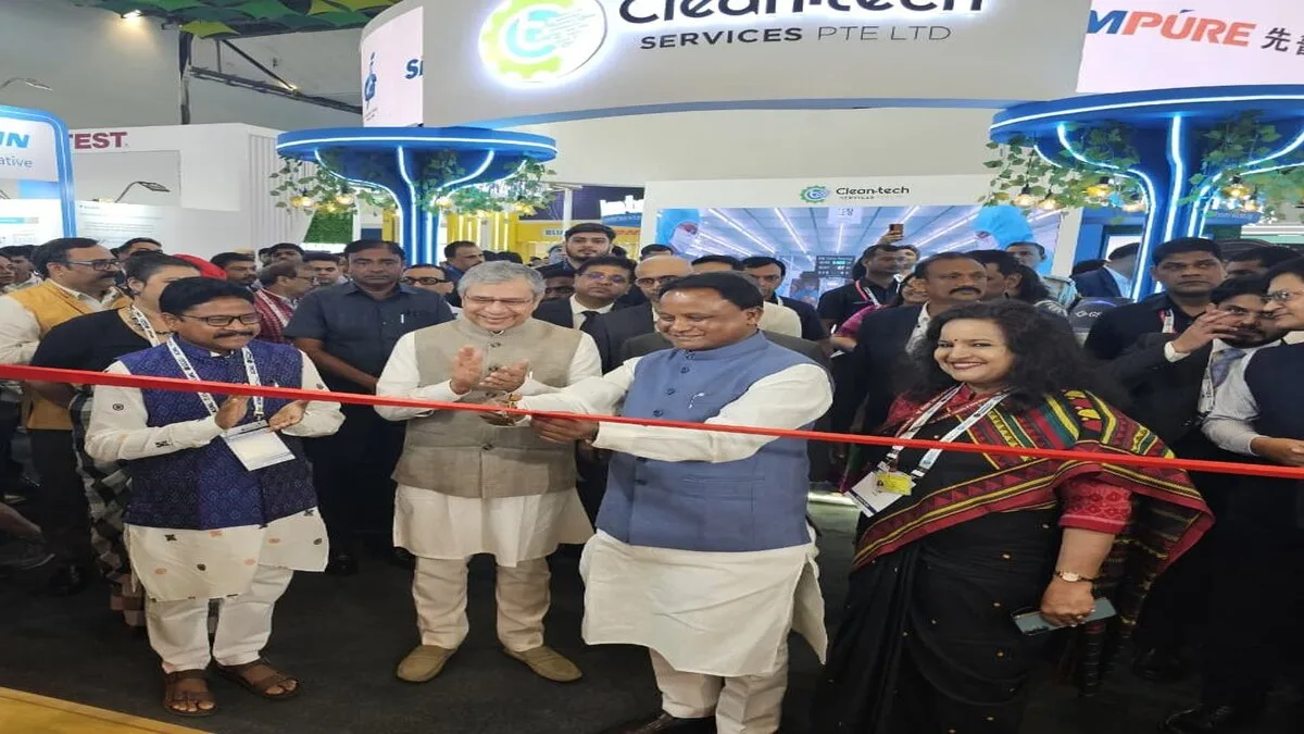
BHUBANESWAR: Odisha has stepped up its efforts to emerge as a major semiconductor and electronics hub, with Chief Minister Mohan Charan Majhi leading high-level engagements with global and domestic technology companies, industry bodies and international delegations at SEMICON India 2026 in New Delhi.
The state government has received investment proposals worth approximately ₹23,600 crore during the engagements, with the proposed investments having the potential to generate around 6,100 employment opportunities. The developments are expected to strengthen Odisha’s semiconductor and electronics ecosystem and support its efforts to build a complete value chain under the India Semiconductor Mission 2.0.
The Chief Minister’s engagements at the industry event focused on attracting new investments, strengthening technology partnerships and creating an ecosystem in which global and Indian companies can establish manufacturing operations, undertake innovation and expand their businesses in Odisha.
Engagement with Global Semiconductor Companies
During SEMICON India 2026, Majhi held discussions with global and domestic semiconductor and technology companies, industry bodies and international delegations.
The engagements included interactions with delegations from Japan, Sweden and Taiwan. The Odisha delegation also held discussions with major companies such as Lam Research, Applied Materials, SiCSem, 3D Glass Solutions, Cyient, Linde and HORIBA India, among others.
The discussions covered investment opportunities, technology, manufacturing capabilities, innovation and the development of supporting infrastructure and skilled manpower.
Semiconductors are shaping the industries of tomorrow, and Odisha is preparing for that future today. With major investments in Silicon Carbide, advanced packaging and power electronics, the State is creating a strong foundation for high-tech manufacturing and quality employment.… pic.twitter.com/GEDCQnVl18
— Mohan Charan Majhi (@MohanMOdisha) September 18, 2026
A major outcome of the engagements was the signing of a Letter of Intent with QuadQuantum for a semiconductor facility for manufacturing silicon carbide (SiC) substrate wafers.
The proposed facility is expected to further strengthen Odisha’s presence in the semiconductor value chain and contribute to the development of an ecosystem around advanced semiconductor materials and technologies.
The state government said the investment proposals and industry engagements represent a further step towards developing an integrated semiconductor and electronics ecosystem rather than focusing only on individual projects.
870-acre Odisha Silicon Valley at Naraj
In a significant infrastructure initiative, Chief Minister Majhi announced the development of an 870-acre Odisha Silicon Valley at Naraj near Cuttack.
The proposed Silicon Valley will accommodate major semiconductor, electronics and information technology projects and is envisaged as a strategic industrial hub for technology-driven growth in the state.
Odisha is steadily building the foundation to become Eastern India’s Silicon Valley.
With an 870-acre dedicated land bank at Naraj, Cuttack, integrated infrastructure and strong multimodal connectivity, we are creating a future-ready ecosystem for semiconductor manufacturing and… pic.twitter.com/2MQNeuSx93
— Mohan Charan Majhi (@MohanMOdisha) September 18, 2026
Naraj offers several locational advantages because of its proximity to the Cuttack-Bhubaneswar urban corridor and its connectivity with major national highways. The location also provides access to important ports, including Paradip and Dhamra, facilitating multimodal movement of industrial equipment, raw materials and finished products.
The government has identified these connectivity advantages as important for the development of semiconductor supply chains, logistics and allied industries.
Odisha is building the semiconductor ecosystem of tomorrow.
With support across the entire semiconductor value chain, from advanced manufacturing and packaging to raw materials, supply chains, talent and chip design, Odisha is creating the foundation for a future-ready… pic.twitter.com/EW70wxjj11
— CMO Odisha (@CMO_Odisha) September 18, 2026
The availability of reliable water and power is also a critical consideration for semiconductor fabrication and assembly facilities. The proposed site’s proximity to the Mahanadi River provides a potential advantage in meeting industrial water requirements.
Combined with its connectivity to urban centres, highways and ports, as well as its infrastructure potential, Naraj is being positioned as the location for developing a world-class semiconductor and electronics ecosystem in Odisha.
‘From intent to implementation’
Speaking about Odisha’s semiconductor journey, Chief Minister Majhi said the state was moving rapidly from investment intent towards implementation.
“Odisha’s semiconductor journey is moving rapidly from intent to implementation. We have been able to attract investments across critical areas of the semiconductor value chain and, importantly, move key projects towards execution,” he said.
Majhi said the discussions with industry leaders at SEMICON India 2026 were focused on sustaining the momentum and attracting the next set of semiconductor investments to Odisha.
“At SEMICON India 2026, our discussions with industry leaders are focused on taking this momentum forward and bringing the next set of semiconductor investments to Odisha. We want to build an ecosystem where global and Indian technology companies can manufacture, innovate and grow,” he said.
The Chief Minister’s remarks underline the state government’s approach of developing an ecosystem that brings together manufacturing, technology, research, innovation, skilled manpower and supporting industries.
Odisha pavilion showcases emerging semiconductor ecosystem
Odisha is showcasing its semiconductor capabilities and investment opportunities at its pavilion at SEMICON India 2026.
The Odisha Pavilion was inaugurated at Yashobhoomi, New Delhi, by Chief Minister Majhi in the presence of Union Minister for Electronics and Information Technology Ashwini Vaishnaw.
Hon’ble Chief Minister Shri @MohanMOdisha inaugurated the Odisha Pavilion at Yashobhoomi, New Delhi, in the presence of Hon’ble Union Minister Shri @AshwiniVaishnaw Ji.
The pavilion brings Odisha’s semiconductor proposition to the forefront, showcasing key projects, policy… pic.twitter.com/xewLte7bo2
— CMO Odisha (@CMO_Odisha) September 18, 2026
The pavilion highlights Odisha’s semiconductor proposition, including key projects, policy incentives, infrastructure and investment opportunities across semiconductor manufacturing, advanced packaging, chip design and electronics.
Projects associated with RIR Power, SiCSem, 3D Glass Solutions and ARF Design are among the initiatives showcased at the pavilion.
The state is also highlighting the contribution of educational and technical institutions in semiconductor design and innovation. Institutions including NIT Rourkela and PMEC, Brahmapur, are working towards the development and design of Made-in-India chips.
The pavilion therefore seeks to present Odisha’s semiconductor ambitions as extending beyond manufacturing to include chip design, research, innovation, technical education and development of specialised talent.
‘Sand to Silicon’ connects Odisha’s industrial past with technology future
A distinctive feature of the Odisha Pavilion is the “Sand to Silicon” installation, which presents the state’s semiconductor journey through an Odisha-specific narrative.
The installation connects Odisha’s industrial identity and natural resources with its emerging ambitions in silicon and advanced technologies.
The concept is also linked to the state’s broader vision of moving from a “Mine Economy” to a “Mind Economy”, with greater emphasis on knowledge, technology, innovation and skilled human resources.
Through the concept, Odisha is seeking to present its semiconductor push as part of a larger transformation of the state’s industrial economy, combining its existing industrial strengths with emerging technology-driven sectors.
Policy aligned with India Semiconductor Mission 2.0
Alongside investment promotion and infrastructure development, Odisha has been expanding its policy support for the semiconductor industry.
The state has positioned itself among the early movers in aligning its Semiconductor Policy with the evolving India Semiconductor Mission 2.0. Its recent Third Policy Amendment has expanded support to several critical segments of the semiconductor value chain.
Under the amended framework, Odisha has extended an additional 25 per cent fiscal support to ISM-approved projects in semiconductor equipment manufacturing, semiconductor-grade gases, raw materials and supply-chain segments.
The policy also provides support for engineer relocation, manpower skilling, internships, international patents and research and development activities.
The government’s objective is to develop a wider ecosystem capable of supporting semiconductor manufacturing while also attracting companies involved in equipment, materials, gases, supply-chain services, research and technology development.
Focus on semiconductor ecosystem, not isolated projects
Odisha Electronics and Information Technology Minister Dr Mukesh Mahaling said the state was focusing on building a complete ecosystem around semiconductor investments.
“Our approach is to build the ecosystem around semiconductor investments, not look at projects in isolation,” Mahaling said.
He said Odisha had taken an early approach towards aligning its policy framework with ISM 2.0 while widening support to equipment, materials, gases and supply-chain activities.
“Alongside this, we are investing in specialised talent and creating the conditions that companies need to set up and scale their operations in the state,” he said.
The government has identified specialised manpower and technical skills as important requirements for attracting and retaining semiconductor companies and enabling them to expand operations in the state.
CM holds discussion with Ashwini Vaishnaw
On the sidelines of SEMICON India 2026, Chief Minister Majhi also held discussions with Union Minister Ashwini Vaishnaw on strengthening Odisha’s semiconductor ecosystem.
Had a discussion with Hon’ble Union Minister for Electronics & Information Technology Shri Ashwini Vaishnaw Ji on the sidelines of SEMICON India 2026 in New Delhi.
We discussed the way forward for strengthening Odisha’s semiconductor ecosystem, with a focus on investment,… pic.twitter.com/rvgejRMywl
— Mohan Charan Majhi (@MohanMOdisha) September 18, 2026
In a social media post, Majhi said the discussion focused on the way forward for strengthening the state’s semiconductor ecosystem, particularly in the areas of investment, technology, innovation and skill development.
The Chief Minister said Odisha remained committed to building a robust semiconductor and electronics ecosystem and contributing meaningfully to the vision of Aatmanirbhar Bharat.
The meeting comes at a time when Odisha is seeking to align its semiconductor initiatives with the national mission and attract investments across multiple stages of the semiconductor value chain.
Positioning Odisha in India’s semiconductor growth story
The investment proposals received at SEMICON India 2026, the proposed 870-acre Odisha Silicon Valley at Naraj, the QuadQuantum Letter of Intent and the expansion of policy incentives constitute key elements of Odisha’s semiconductor strategy.
The state is seeking to create an ecosystem spanning semiconductor manufacturing, advanced packaging, chip design, electronics, equipment, raw materials, specialised gases, research and development and supply-chain activities.
The government is also emphasising skilled employment and stronger industry-academia linkages to create the specialised talent base required by the sector.
With its proposed Silicon Valley at Naraj, connectivity to major ports and urban centres, expanded policy incentives and growing engagement with global technology companies, Odisha is presenting itself at SEMICON India 2026 as an emerging destination for semiconductor and electronics investments.
The state is positioning the initiative within its broader vision of building a knowledge- and technology-driven economy and contributing to India’s semiconductor growth and the objective of Aatmanirbhar Bharat.
![Vav-Tharad [Gujarat], Mar 31 (ANI): Prime Minister Narendra Modi during the laying of the foundation stone and inauguration of multiple development projects, in Vav-Tharad on Tuesday. Gujarat Chief Minister Bhupendra Patel, State Deputy Chief Minister Harsh Sanghavi and others also present. (DPR PMO/ANI Photo)](https://organiser.org/wp-content/uploads/2026/04/20260331377l-1-120x86.webp)