




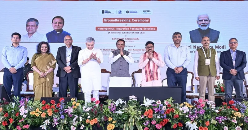
Bhubaneswar: In a landmark development for India’s semiconductor ambitions, the foundation stone for the country’s first advanced 3D semiconductor packaging unit was laid at Info Valley in Bhubaneswar, positioning Odisha as a key player in the global electronics and semiconductor value chain. The project marks a decisive step toward strengthening domestic manufacturing capabilities and advancing the vision of self-reliance in high-end electronics.
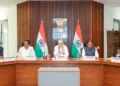
The Heterogeneous Integration Packaging Solutions project, promoted by 3D Glass Solutions, was inaugurated in the presence of Chief Minister Mohan Charan Majhi and Union Minister for Railways, Electronics & IT, and Information & Broadcasting Ashwini Vaishnaw. With this initiative, Odisha is set to host one of the world’s most advanced chip packaging technologies, further cementing its emergence as a future-ready technology hub.
Addressing the gathering, Chief Minister Majhi described the project as a historic milestone for both the state and the nation. He highlighted that for the first time in India, such an advanced 3D glass substrate-based semiconductor packaging facility is being established, bringing significant pride to Odisha. He noted that global technology leaders such as Intel, Lockheed Martin, and Applied Materials are associated with cutting-edge semiconductor technologies, and their growing engagement signals increasing global confidence in Odisha’s industrial ecosystem.
Today, from the soil of Odisha, India took a defining step in its semiconductor journey. I was delighted to join Hon'ble Union Minister Shri @AshwiniVaishnaw Ji for the groundbreaking ceremony of the nation's first advanced 3D glass substrate packaging facility, a historic… pic.twitter.com/ruDUsn6rHm
— Mohan Charan Majhi (@MohanMOdisha) April 19, 2026
The Chief Minister emphasised that the products manufactured at the facility will play a crucial role in next-generation sectors, including artificial intelligence, high-performance computing, defence electronics, telecommunications, and advanced digital systems. He reiterated that Odisha is well-positioned to contribute significantly to Prime Minister Narendra Modi’s vision of making India self-reliant in semiconductor and electronics manufacturing under the broader “Atmanirbhar Bharat” initiative.
This facility will generate thousands of quality jobs for our youth and anchor a thriving ecosystem of testing laboratories and ancillary industries, accelerating Odisha's transformation from a mineral-driven economy to a mind-driven one, where the brilliance of Odia talent meets… pic.twitter.com/cGEevV6nuA
— Mohan Charan Majhi (@MohanMOdisha) April 19, 2026
Providing details of the investment, Majhi stated that the project involves an outlay of nearly ₹2,000 crore. Once operational, the facility is expected to produce approximately 70,000 glass panels annually, along with 50 million assembled units and around 13,000 advanced 3D heterogeneous integration (3DHI) modules. He further noted that Odisha has emerged as a unique destination in India where both the country’s first compound semiconductor fabrication unit and its first 3D glass substrate packaging facility are being established.
Highlighting the economic impact, the Chief Minister said the rapidly growing semiconductor ecosystem in the state will generate substantial employment opportunities for engineering graduates, diploma holders, and ITI students. This transformation is expected to shift Odisha’s economic profile from a resource-driven model to a technology-led growth hub.
Union Minister Ashwini Vaishnaw, while addressing the event, congratulated the people of Odisha and commended the state government for its proactive support in facilitating such high-value investments. He observed that under the leadership of Prime Minister Narendra Modi, India’s semiconductor sector is witnessing unprecedented growth, with Odisha emerging as a significant contributor to this transformation.
World’s most advanced semiconductor technology comes to Odisha.
Groundbreaking of India’s first 3D Glass Chip Packaging Unit, along with Odisha CM @MohanMOdisha Ji. pic.twitter.com/4cpBGj9Iky
— Ashwini Vaishnaw (@AshwiniVaishnaw) April 19, 2026
Vaishnaw noted that Odisha, traditionally known for its strengths in minerals, metals, and energy, is now steadily diversifying into advanced sectors such as electronics, information technology, and semiconductors. He described the project as one of the most sophisticated manufacturing initiatives in the country, capable of strengthening India’s semiconductor value chain and reducing dependence on imports.
Speaking about the broader progress in electronics manufacturing, the Union Minister highlighted that India’s production in the sector has grown six-fold over the past 12 years. He added that the country has become the world’s second-largest mobile phone manufacturer and emerged as a leading exporter of mobile phones in 2025, underscoring the rapid evolution of India’s electronics ecosystem.
Vaishnaw also revealed that two semiconductor projects have already been approved for Odisha under the India Semiconductor Mission, with three more proposals currently under consideration. He mentioned that discussions are ongoing with major global players, including Intel, for future investments in the state, indicating sustained interest from international technology firms.
In addition to semiconductor developments, the Union Minister outlined major advancements in railway infrastructure across Odisha. He stated that projects worth over ₹90,000 crore are currently under execution, reflecting a significant expansion of rail connectivity. The state has received a record railway budget allocation of ₹10,928 crore, while 59 stations are being redeveloped under the Amrit Bharat Station Scheme.
He further informed that efforts are underway to connect all 30 districts of Odisha through an expanded railway network. Key initiatives include the proposed four-line coastal rail corridor from Balasore to Berhampur, which is expected to enhance both freight and passenger movement. Vaishnaw emphasised that these infrastructure projects will boost regional connectivity, facilitate economic growth, and integrate Odisha more closely with national logistics networks.
Reaffirming the government’s commitment, he stated that railway infrastructure development in the state will continue to focus on speed, safety, and passenger comfort, ensuring balanced and inclusive growth across all regions.
State Electronics & IT Minister Dr Mukesh Mahaling also addressed the gathering, stating that Odisha is rapidly emerging as a semiconductor hub. He highlighted that the state’s progressive policies, including IT, AI, GCC, and Semiconductor Policies 2025, are designed to attract investments and foster innovation.
Emphasising skill development, Mahaling said the government is providing stipend support to engineering students to build an industry-ready workforce. He added that initiatives such as the Blackswan Summit 2026 and increasing investments in artificial intelligence will further strengthen Odisha’s position in future technologies and create new employment opportunities.
The project is being implemented by 3D Glass Solutions Inc., USA, through its wholly owned Indian subsidiary Heterogeneous Integration Packaging Solutions Pvt. Ltd. at Info Valley in Khordha district. It is a greenfield, vertically integrated advanced packaging and embedded glass substrate assembly, testing, marking, and packaging (ATMP) facility.
The total project cost is estimated at ₹1,943.53 crore, which includes central government fiscal support of ₹799 crore and additional state support of approximately ₹399.5 crore. The facility is designed to cater to high-growth sectors such as data centres, artificial intelligence, machine learning, 5G and 6G communications, automotive radar, defence electronics, aerospace applications, and photonics.
Commercial production at the unit is expected to commence by August 2028, while full-scale volume production is targeted by August 2030.