





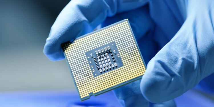
Odisha: UK firm plans 800-Acre Semiconductor Unit worth Rs 2 Lakh Crore
July 14, 2026
  • Read Ecopy
  • Circulation
  • Advertise
  • Careers
  • About Us
  • Contact Us
Android AppiPhone AppArattai
Organiser
  • ‌
  • Bharat
    • Assam
    • Bihar
    • Chhattisgarh
    • Jharkhand
    • Maharashtra
    • View All States
  • World
    • Asia
    • Europe
    • North America
    • South America
    • Africa
    • Australia
  • Editorial
  • International
  • Opinion
  • RSS @ 100
  • More
    • Op Sindoor
    • Analysis
    • Sports
    • Defence
    • Politics
    • Business
    • Economy
    • Culture
    • Special Report
    • Sci & Tech
    • Entertainment
    • G20
    • Azadi Ka Amrit Mahotsav
    • Vocal4Local
    • Web Stories
    • Education
    • Employment
    • Books
    • Interviews
    • Travel
    • Law
    • Health
    • Obituary
  • Subscribe
    • Subscribe Print Edition
    • Subscribe Ecopy
    • Read Ecopy
  • ‌
  • Bharat
    • Assam
    • Bihar
    • Chhattisgarh
    • Jharkhand
    • Maharashtra
    • View All States
  • World
    • Asia
    • Europe
    • North America
    • South America
    • Africa
    • Australia
  • Editorial
  • International
  • Opinion
  • RSS @ 100
  • More
    • Op Sindoor
    • Analysis
    • Sports
    • Defence
    • Politics
    • Business
    • Economy
    • Culture
    • Special Report
    • Sci & Tech
    • Entertainment
    • G20
    • Azadi Ka Amrit Mahotsav
    • Vocal4Local
    • Web Stories
    • Education
    • Employment
    • Books
    • Interviews
    • Travel
    • Law
    • Health
    • Obituary
  • Subscribe
    • Subscribe Print Edition
    • Subscribe Ecopy
    • Read Ecopy
Organiser
  • Home
  • Bharat
  • World
  • Operation Sindoor
  • Editorial
  • Analysis
  • Opinion
  • Culture
  • Defence
  • International Edition
  • RSS @ 100
  • Magazine
  • Read Ecopy
Home Bharat

Odisha: UK firm plans 800-Acre Semiconductor Unit worth Rs 2 Lakh Crore

The company's project director, Debadutt Singhdeo, stated, "The company has aimed to establish the unit within two years and to provide direct employment to 5,000 people. It has also planned to expand the unit in subsequent phases by investing around Rs 2 lakh crore by 2027".

WEBDESKWEBDESK
Jul 1, 2023, 10:00 pm IST
in Bharat, Odisha
Follow on Google News
FacebookTwitterWhatsAppTelegramEmail

UK-based corporation SRAM & MRAM Group intends to set up a huge semiconductor fabrication unit in the Ganjam district, Odisha. The first phase to establish this unit will be started with an initial investment of Rs 30,000 crore. The project’s total cost is estimated to be over Rs 2 lakh crore.

The UK-based SRAM & MRAM Group’s Indian division SRAM & MRAM Technologies and Projects India Pvt Limited inked a memorandum of understanding (MoU) with the state government to establish the semiconductor plant in Odisha. This MoU was signed on March 26, and now the officials from the company are on a field visit to decide upon the factory’s location in the Ganjam district.

On June 29, after inspecting certain sites in the district near Chhatrapur, its Indian firm representatives, led by its chairman Guruji Kumaran Swami, met with the district administration in Chhatrapur. The District Collector of Ganjam Dibya Jyoti Parida has informed the investors that the administration will provide all necessary facilities for the establishment of the semiconductor unit.

The company’s project director, Debadutt Singhdeo, said, “We have visited some sites, including the industrial park of Tata and some private lands for the establishment of the proposed semiconductor unit. A technical team of the company will visit the district to finalise the site”. The corporation will need up to 800 acres of land to build the unit.

Even though company representatives also travelled to other districts, they chose the location near Chhatrapur because it was close to the Gopalpur port, a designated industrial corridor, an airstrip, and a national highway, in addition to having access to clean water and energy, which are essential for the fabrication unit.

Singhdeo stated, “The company has aimed to establish the unit within two years and to provide direct employment to 5,000 people. It has also planned to expand the unit in subsequent phases by investing around Rs 2 lakh crore by 2027”.

Also Read: US chip-maker Micron signs MoU worth Rs 22,500 crore with Gujarat Government

This new facility in Odisha will boost India’s Semiconductor Mission. It will boost India’s ambition to become a global electronics manufacturing and design hub. In the manufacturing of modern electronics, semiconductors are critical components in it. From autos and medical equipment to smartphones and laptops, they are utilised in various products to make integrated circuits, memory modules, and microprocessors in these products.

Recently following the approval of the proposal of US-based chip-maker Micron to set up a 2.7 billion dollar semiconductor testing and packaging unit by the Government of India, the Gujarat government signed a pact with Micron on June 28 worth Rs 22,500 crore to set up an ATMP (assembly, test, marking, and packaging) facility at Sanand city, which comes under Ahmedabad district.

During the meeting of Micron with the Gujarat government, both stakeholders signed an MoU to establish an assembly and test facility at Sanand GIDC. The MoU was signed between the Secretary of the Department of Science and Technology, Vijay Nehra, and the Senior Vice President of Micron Gursharan Singh.

Vice Chairman and Managing Director, GIDC handed over the Offer Cum Allotment (OCA) letter to Micron for the allotment of 93 acres of area within the Sanand GIDC Estate. As per the release by the Gujrat government, Micron will establish Assembly and Test facility, which will focus on transforming wafers into ball grid array (BGA) integrated circuit packages, memory modules and solid-state drives.

Micron is committed to designing and building the facility to meet or exceed leadership in Energy and Environmental Design (LEED) Gold standards. Additionally, the facility will use advanced water-saving technologies to enable Zero Liquid Discharge (ZLD).


 

Topics: Semiconductor MissionSRAM & MRAM Groupsemiconductor fabrication unitGanjamDebadutt Singhdeo
Share1TweetSendShareSend
✮ Subscribe Organiser YouTube Channel. ✮
✮ Join Organiser's WhatsApp channel for Nationalist views beyond the news. ✮
Previous News

USA: Supreme Court scraps racial and colour-based discriminatory admission policies in Universities

Next News

Diet tracking is essential for effective weight loss: Study

Related News

PM Modi at Micron Technology’s Semiconductor ATMP facility

All you need to know about India’s first domestic semiconductor chip facility inaugurated by PM Modi in Sanand

'This Decade Is India's Tech-ade': PM Modi Inaugurates Semiconductor Plant In Greater Noida | Image: X

“Made in India chips key to self-reliance”: PM Modi launches semiconductor facility in Greater Noida

Taiwan Semiconductor Manufacturing Corporation (TSMC)

Taiwanese tech firms consider relocating manufacturing bases to India amid rising tensions

From Left: Chief Minister K Chandrashekar Rao, Foxconn chairman Young Liu and KT Rama Rao, Telangana's Minster of Industries and Commerce

Telangana: Apple’s supplier Foxconn increases investment in India; to set up a USD 500 million manufacturing unit

Load More

Latest News

J&K unit of BJP has filed the defamation case against the CM Omar Abdullah

J&K: BJP serves Rs 100-crore defamation notice to CM Omar for making allegations of bribery to NC legislators

(Left) CDS Gen N S Raja Subramani (Right) Union Defence Minister Rajnath Singh

Bharat’s bold leap towards Integrated Theatre Commands: CDS Gen Subramani pushes historic military reform

A delegation of Hindu Aikyavedi met Chief Minister VD Satheeshan

Keralam: Hindu Aikyavedi delegation meets CM, submits resolutions adopted at Hindu leadership conclave

IED blast targets Assam Rifles Convoy in Nagaland; One martyred

IED attack on Assam Rifles convoy in Nagaland; One soldier martyred, four injured; CM Rio terms it cowardly act

Representative Image

PoJK protests hit White House as Kashmiri diaspora shouts anti-Pakistan slogans; Muzaffarabad rises against abuse

Home Minister Amit Shah laying foundation stone for 125-foot Dr Syama Prasad Mookerjee statue in Kolkata

Dr Syama Prasad Mookerjee: Not just a statue but the foundation of Sonar Bangla

Indian mathematician T A Sarasvati Amma

The Woman Who Rewrote Mathematical History: The extraordinary journey of T A Sarasvati Amma

The people in Pakistan-occupied Jammu Kashmir (PoJK) are rising against Pakistan's brutality

POJK Unrest: Azad or gulam

Prime Minister Narendra Modi (Left) and Indonesian President Prabowo Subianto (Right)

PM Modi’s Indonesia Visit: Threads from the past, transformation for future

PoJK: Uprising against continued colonisation

Load More
  • Privacy
  • Terms
  • Cookie Policy
  • Refund and Cancellation
  • Delivery and Shipping

© Bharat Prakashan (Delhi) Limited.
Tech-enabled by Ananthapuri Technologies

  • Home
  • Search Organiser
  • Bharat
    • Assam
    • Bihar
    • Chhattisgarh
    • Jharkhand
    • Maharashtra
    • View All States
  • World
    • Asia
    • Africa
    • North America
    • South America
    • Europe
    • Australia
  • Editorial
  • Operation Sindoor
  • Opinion
  • Analysis
  • Defence
  • Culture
  • Sports
  • Business
  • RSS @ 100
  • Entertainment
  • More ..
    • Sci & Tech
    • Vocal4Local
    • Special Report
    • Education
    • Employment
    • Books
    • Interviews
    • Travel
    • Health
    • Politics
    • Law
    • Economy
    • Obituary
  • Subscribe Magazine
  • Read Ecopy
  • Advertise
  • Circulation
  • Careers
  • About Us
  • Contact Us
  • Policies & Terms
    • Privacy Policy
    • Cookie Policy
    • Refund and Cancellation
    • Terms of Use

© Bharat Prakashan (Delhi) Limited.
Tech-enabled by Ananthapuri Technologies