





Long before the word “innovation” entered common usage, India was already living it. In the furnaces of ancient India, metallurgists forged Wootz steel of such purity that European swordsmiths would spend a thousand years failing to replicate its edge. In the observatories of Ujjain, astronomers calculated planetary motion with instruments carved from stone and brass, centuries ahead of their European counterparts.
And in the scriptoria of Nalanda and Takshashila, mathematicians gave the world the concept of zero the silent digit without which no computation, ancient or digital, could ever exist. India’s history is not one of borrowed ingenuity but of civilisational firsts, quietly authored millennia before Silicon Valley had a name. Today, in fabless design studios from Chennai to Bengaluru, a new generation of Indian engineers is carving equally invisible, equally consequential inventions not in steel or stone, but in silicon. It is, in many ways, the same old civilisational instinct at work to conceive what the world has not yet imagined and to build it with quiet mastery.
Design: The silent architect of value
Semiconductor chip design rarely makes headlines the way a finished smartphone or an electric vehicle does, yet it is the single most valuable link in the entire semiconductor chain. Design contributes up to 50 per cent of the overall value addition in a chip and accounts for roughly 15 to 35 per cent of the Bill of Materials cost of the electronic products it powers.
If fabrication is the forge, design is the architects blueprint the layer where intelligence, efficiency and strategic advantage are actually created. For decades, that blueprint was drawn almost entirely outside India, even as Indian engineers staffed the design floors of global semiconductor giants from California to Bengaluru’s own outsourced campuses. The strategic question was never whether Indian talent could design world-class chips that had long been proven inside foreign firms but the question is whether India could design and commercialise them as a nation.
Recognising this the Government of India Design Linked Incentive (DLI) Scheme has been steadily building a nursery of Indian startups capable of designing chips for satellite communications, drones, surveillance systems, defence and aerospace platforms, automotive electronics, the Internet of Things, LED drivers, artificial intelligence systems, telecom equipment and smart meters.
It is a deliberate bet that the country which once gave the world zero can also give it the next generation of silicon intelligence and that in an era where semiconductor supply chains have become instruments of geopolitical leverage, self-reliance in chip design is no longer optional, but foundational to the vision of a Viksit Bharat by 2047.
Aheesa Digital Innovations: A Chennai startup’s VIHAAN moment
Among the clearest signs that this bet is paying off is the story of Aheesa Digital Innovations, a Chennai-headquartered fabless semiconductor startup specialising in chips for broadband networking and security. Aheesa flagship product, VIHAAN, is a networking System-on-Chip purpose-built for fibre broadband. The chip journey carries a symbolism that would not be lost on any student of the calendar it was taped out on Republic Day and achieved first-pass silicon success on Independence Day this year.
VIHAAN will now proceed towards production tape-out, targeted for 2027. As India expands its digital backbone through optical fibre, 5G and broadband-led services, the demand for domestically designed semiconductor solutions is only growing and Aheesa, through the VIHAAN series and the scaffolding of the DLI Scheme, is positioning itself to meet that demand from within India rather than importing it.
Investor Confidence: Betting on India’s deep-tech future
Capital tends to follow conviction and conviction is precisely what Aheesa has attracted. Earlier this year, the company raised close to ₹40 crore from TNIFMC through the Tamil Nadu Emerging Sector Seed Fund, alongside other private investors, to accelerate product development and scale its presence in the semiconductor space. That this funding arrived after Aheesa’s approval under the DLI Scheme is telling government backing did not crowd out private capital, it catalysed it.
Investors are increasingly willing to back Indian deep-tech ventures capable of delivering advanced broadband silicon solutions designed, tested and refined on Indian soil a marker of growing global confidence in India’s semiconductor design capabilities, not merely its manufacturing potential. This pattern a government incentive de-risking the earliest, most uncertain stage of deep-tech product development, followed by private capital stepping in once technical feasibility is demonstrated is precisely the kind of public-private sequencing that mature semiconductor economies have relied on for decades.
That India is now replicating it, at speed and at scale, suggests the DLI Scheme is functioning less as a subsidy and more as a signal to global venture capital that Indian silicon is investable.
From Idea to Product: The ecosystem the government has built
Aheesa’s rise is not an isolated success story, it is one visible outcome of a much larger transformation underway in Indian semiconductor design ecosystem. Through the Government semiconductor programmes, state-of-the-art chip-design tools have been made available to 455 organisations, including 350 academic institutions and 105 startups, allowing students, researchers and companies across the country to design chips that were, until recently, the exclusive preserve of a handful of global technology hubs.
Companies supported under the DLI Scheme have together achieved more than 30 chip design tape-outs across various foundries and raised over US$100 million in venture capital funding a clear indicator of investor confidence in India’s semiconductor design capabilities. Alongside this, the Chips to Startup (C2S) Programme has enabled 245 chip designs to be taped out by 71 academic institutions, a pipeline built explicitly to meet the workforce requirements of tomorrow semiconductor industry.
Together, these numbers describe something more significant than any single scheme with a systematic effort to move Indian talent from the classroom to the cleanroom, from the whiteboard to working silicon. For a country whose engineering colleges have long produced world-class talent for other nation semiconductor industries, the availability of design tools within India’s own institutions marks a quiet but consequential shift the skills no longer need to travel abroad to find a chip worth designing.
Other recent successes under the scheme
Aheesa is far from alone. In recent months, several other DLI-supported companies have reached notable technical milestones of their own, each adding another chip to India’s growing semiconductor design capability.
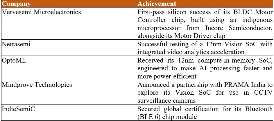
Each of these achievements, modest as it may appear in isolation, represents a chip that once would almost certainly have been designed abroad. Taken together, they sketch the outline of an ecosystem that is no longer merely aspiring to design silicon, but is routinely doing so.
Semicon 2.0: The vision of Viksit Bharat
The Government’s semiconductor initiatives were never conceived as a scheme to design isolated chips, the ambition has always been to build an entire ecosystem spanning chip design and manufacturing, advanced packaging, equipment, materials, research, development and skilled manpower. With Semicon 2.0, approved with an outlay of ₹1,27,500 crore in July 2026, India is taking this effort to its next stage, with the explicit objective of building a globally competitive semiconductor ecosystem rather than a collection of standalone successes.
The progress of companies such as Aheesa Digital Innovations demonstrates that Indian semiconductor designs are increasingly moving beyond the laboratory. Chips conceived in Indian design studios are now being fabricated, tested, validated and readied for customer trials abroad and at home. As the ecosystem matures further, these silicon-validated designs are expected to move towards volume manufacturing, positioning Indian companies as credible global suppliers while simultaneously strengthening the country domestic supply chains and technological self-reliance.
It is worth pausing on what this moment represents. The India that once gave the world the zero, that shaped steel no furnace in Europe could match, and that mapped the heavens with instruments of stone, is now designing the silicon brains of tomorrow’s satellites, vehicles and communication networks. The tools have changed beyond recognition the cleanroom has replaced the smithy, and the design workstation has replaced the observatory but the underlying instinct has not.
It is the same civilisational confidence that once turned raw ore into steel of legend, now turning raw silicon into sovereign intelligence. Vikas Bhi, Virasat Bhi development and heritage walking hand in hand finds in this story one of its most literal expressions for an ancient nation of mathematicians and metallurgists using the twenty-first century defining material to write its next chapter. In Chennai fabless studios and in the DLI Schemes expanding list of successes, that ancient instinct has simply found its newest, smallest and most consequential canvas one measured not in cubits or carats but in nanometres.