
India has made significant progress in developing a skilled semiconductor workforce as part of its broader strategy to strengthen domestic chip design and manufacturing capabilities.
Union Minister for Electronics and Information Technology Ashwini Vaishnaw highlighted the progress while discussing the government’s talent development initiative under the Chips to Startups programme, a key component of the India Semiconductor Mission.
According to the minister, the programme is steadily advancing toward its ten-year goal of training 85,000 semiconductor design engineers, a crucial step for India’s ambition to become a major player in the global semiconductor ecosystem.
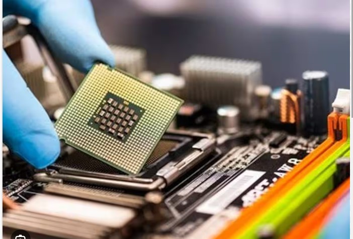
The initiative focuses on training students in semiconductor design by providing access to advanced Electronic Design Automation (EDA) tools, software platforms used by engineers to design and test semiconductor chips.
These tools have been supplied by leading global technology companies including Synopsys, Cadence Design Systems, Siemens, Renesas Electronics, Ansys, and AMD.
Currently, these platforms have been deployed across 315 academic institutions throughout India, enabling engineering students to gain practical exposure to semiconductor design.
Officials say this access allows students to work on real chip design projects using the same tools employed by global semiconductor companies.
Under the programme, students not only design semiconductor chips but also gain exposure to the entire chip development cycle.
The designs created by students are subsequently fabricated and tested at the **Semiconductor Laboratory in Mohali, providing hands-on experience across key stages of the semiconductor value chain.
This includes: Chip design, Fabrication, Packaging and Testing.
Such exposure helps students understand how theoretical design concepts translate into real-world semiconductor production.
Officials say the initiative has evolved into the world’s largest open-access Electronic Design Automation training programme.
So far, students participating in the programme have recorded more than 1.85 crore hours of EDA tool usage, indicating high engagement levels across engineering institutions.
The programme has also achieved a nationwide footprint, with students from institutions across India—from Assam and Gujarat to Kashmir and Kanyakumari—actively participating in semiconductor design projects.
This wide geographical participation reflects the government’s aim to build semiconductor talent across the country rather than concentrating it in a few technology hubs.
The government is planning a further expansion of the programme under the upcoming India Semiconductor Mission 2.0.
Under the new phase, the number of participating academic institutions will increase from 315 to 500, significantly expanding the talent pipeline for semiconductor design and related fields.
Officials believe that this expansion will help India create a larger pool of engineers capable of contributing to the semiconductor ecosystem, including chip design, fabrication, and advanced electronics manufacturing.
The push to develop semiconductor talent comes at a time when the global semiconductor industry is projected to grow rapidly.
Industry estimates suggest that the global market—currently valued at around $800–900 billion—could reach nearly $2 trillion in the coming years.
With rising demand for advanced chips powering technologies such as artificial intelligence, electric vehicles, telecommunications, and consumer electronics, governments around the world are investing heavily in semiconductor manufacturing and research.
Indian policymakers believe that by investing early in talent development, the country can position itself as a key contributor to the global semiconductor supply chain.
The expansion of the semiconductor training programme also aligns with India’s broader strategy to strengthen technological self-reliance.
By building a large pool of skilled chip designers and engineers, the government hopes to attract global semiconductor companies to invest in India while also encouraging domestic innovation in chip design and electronics manufacturing.
Officials say that initiatives such as the India Semiconductor Mission are expected to play a crucial role in shaping the country’s future as a major technology and manufacturing hub.