




India Semiconductor push, India plans to train 85,000 designers
September 13, 2026
  • Read Ecopy
  • Circulation
  • Advertise
  • Careers
  • About Us
  • Contact Us
Android AppiPhone AppArattai
Organiser
  • ‌
  • Bharat
    • Assam
    • Bihar
    • Chhattisgarh
    • Jharkhand
    • Maharashtra
    • View All States
  • World
    • Asia
    • Europe
    • North America
    • South America
    • Africa
    • Australia
  • Editorial
  • International
  • Opinion
  • RSS @ 100
  • More
    • World Hindu Congress 2026
    • Op Sindoor
    • Analysis
    • Sports
    • Defence
    • Politics
    • Business
    • Economy
    • Culture
    • Special Report
    • Sci & Tech
    • Entertainment
    • G20
    • Azadi Ka Amrit Mahotsav
    • Vocal4Local
    • Web Stories
    • Education
    • Employment
    • Books
    • Interviews
    • Travel
    • Law
    • Health
    • Obituary
  • Subscribe
    • Subscribe Print Edition
    • Subscribe Ecopy
    • Read Ecopy
  • ‌
  • Bharat
    • Assam
    • Bihar
    • Chhattisgarh
    • Jharkhand
    • Maharashtra
    • View All States
  • World
    • Asia
    • Europe
    • North America
    • South America
    • Africa
    • Australia
  • Editorial
  • International
  • Opinion
  • RSS @ 100
  • More
    • World Hindu Congress 2026
    • Op Sindoor
    • Analysis
    • Sports
    • Defence
    • Politics
    • Business
    • Economy
    • Culture
    • Special Report
    • Sci & Tech
    • Entertainment
    • G20
    • Azadi Ka Amrit Mahotsav
    • Vocal4Local
    • Web Stories
    • Education
    • Employment
    • Books
    • Interviews
    • Travel
    • Law
    • Health
    • Obituary
  • Subscribe
    • Subscribe Print Edition
    • Subscribe Ecopy
    • Read Ecopy
Organiser
  • Home
  • Bharat
  • World
  • Operation Sindoor
  • Editorial
  • Analysis
  • Opinion
  • Culture
  • Defence
  • International Edition
  • RSS @ 100
  • Magazine
  • Read Ecopy
Home Bharat

India’s semiconductor push gains momentum: Plan to train 85,000 chip designers expands to 500 institutions

India is accelerating efforts to build a robust semiconductor workforce, with the government moving closer to its target of training 85,000 chip design engineers under the India Semiconductor Mission

WEBDESKWEBDESK
Mar 9, 2026, 09:00 am IST
inBharat
Follow on Google News
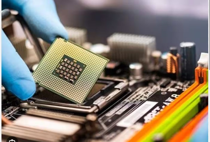
Representative Image

Representative Image

Facebook
Twitter
WhatsAppTelegramEmail

India has made significant progress in developing a skilled semiconductor workforce as part of its broader strategy to strengthen domestic chip design and manufacturing capabilities.

Union Minister for Electronics and Information Technology Ashwini Vaishnaw highlighted the progress while discussing the government’s talent development initiative under the Chips to Startups programme, a key component of the India Semiconductor Mission.

According to the minister, the programme is steadily advancing toward its ten-year goal of training 85,000 semiconductor design engineers, a crucial step for India’s ambition to become a major player in the global semiconductor ecosystem.

The initiative focuses on training students in semiconductor design by providing access to advanced Electronic Design Automation (EDA) tools, software platforms used by engineers to design and test semiconductor chips.

These tools have been supplied by leading global technology companies including Synopsys, Cadence Design Systems, Siemens, Renesas Electronics, Ansys, and AMD.

Currently, these platforms have been deployed across 315 academic institutions throughout India, enabling engineering students to gain practical exposure to semiconductor design.

Officials say this access allows students to work on real chip design projects using the same tools employed by global semiconductor companies.

Under the programme, students not only design semiconductor chips but also gain exposure to the entire chip development cycle.

The designs created by students are subsequently fabricated and tested at the **Semiconductor Laboratory in Mohali, providing hands-on experience across key stages of the semiconductor value chain.

This includes: Chip design, Fabrication, Packaging and Testing.

Such exposure helps students understand how theoretical design concepts translate into real-world semiconductor production.

Officials say the initiative has evolved into the world’s largest open-access Electronic Design Automation training programme.

So far, students participating in the programme have recorded more than 1.85 crore hours of EDA tool usage, indicating high engagement levels across engineering institutions.

The programme has also achieved a nationwide footprint, with students from institutions across India—from Assam and Gujarat to Kashmir and Kanyakumari—actively participating in semiconductor design projects.

This wide geographical participation reflects the government’s aim to build semiconductor talent across the country rather than concentrating it in a few technology hubs.

The government is planning a further expansion of the programme under the upcoming India Semiconductor Mission 2.0.

Under the new phase, the number of participating academic institutions will increase from 315 to 500, significantly expanding the talent pipeline for semiconductor design and related fields.

Officials believe that this expansion will help India create a larger pool of engineers capable of contributing to the semiconductor ecosystem, including chip design, fabrication, and advanced electronics manufacturing.

The push to develop semiconductor talent comes at a time when the global semiconductor industry is projected to grow rapidly.

Industry estimates suggest that the global market—currently valued at around $800–900 billion—could reach nearly $2 trillion in the coming years.

With rising demand for advanced chips powering technologies such as artificial intelligence, electric vehicles, telecommunications, and consumer electronics, governments around the world are investing heavily in semiconductor manufacturing and research.

Indian policymakers believe that by investing early in talent development, the country can position itself as a key contributor to the global semiconductor supply chain.

The expansion of the semiconductor training programme also aligns with India’s broader strategy to strengthen technological self-reliance.

By building a large pool of skilled chip designers and engineers, the government hopes to attract global semiconductor companies to invest in India while also encouraging domestic innovation in chip design and electronics manufacturing.

Officials say that initiatives such as the India Semiconductor Mission are expected to play a crucial role in shaping the country’s future as a major technology and manufacturing hub.
Topics: India Semiconductor Missionchip design training IndiaAshwini Vaishnaw semiconductor programmeChips to Startups initiativesemiconductor workforce India
Share
Tweet
SendShareSend
✮ Subscribe Organiser YouTube Channel. ✮
✮ Join Organiser's WhatsApp channel for Nationalist views beyond the news. ✮
Previous News

Uttam Nagar Murder Case: MCD demolishes property linked to accused in Nizamuddin amid tensions

Next News

Row erupts over President Murmu’s visit to Santal conference: PM Modi slams TMC for ‘Protocol lapses’

Related News

A representative image

Gujarat to set up Rs 190 crore semiconductor hub at IIT Gandhinagar, boosting India’s chip ecosystem

India’s semiconductor roadmap shifts from import dependence to silicon sovereignty, aiming for a self-reliant ecosystem by Viksit Bharat 2047

From Import Dependence to Silicon Sovereignty: India’s bold semiconductor roadmap for Viksit Bharat 2047

India's semiconductor industry treads on path of growth

India launches Indigenous silicon photonics solutions at IIT Madras, boosting semiconductor self-reliance

Representative image

From Import Dependence to Chip Ambition: How Bharat is building a domestic semiconductor ecosystem

A representative image

Make in India gets strategic lift as Apple looks beyond China for iPhone chip assembly in Bharat

Anusandhan National Research Foundation is reshaping the vision of Viksit Bharat@2047 through R&D

Viksit Bharat @ 2047 through strategic research development and innovation initiatives

Load More

Latest News

Exterior of the Lokayukta Building

Karnataka Lokayukta records 1,248 cases in four years, 887 linked to bribery

RSS Akhil Bharatiya Karyakarini Sadasya Dr Manmohan Vaidya at a Pramukh Jan Samvad Sangosthi organised by Kashi Mahanagar on the occasion of the RSS Centenary Year,

Entire society must unite with a sense of oneness; This Is the spirit of Sangh Work: Dr Manmohan Vaidya

‘Samuel Could Never Do This’: Mother Rejects Blasphemy Allegations Against Son in Lahore

Pakistan Blasphemy Case: Mother of Christian man Samuel Arif claims false implication, seeks justice

Prime Minister Narendra Modi, along with Chinese President Xi Jinping, Russian President Vladimir Putin and other world leaders, poses for a picture at a joint tree plantation initiative during the BRICS Summit

BRICS Summit 2026: India as the voice of Global South, shared responsibilities & scripting inclusive world order

Chinese President Xi Jinping and Prime Minister Narendra Modi

BRICS Summit 2026: PM Modi hold talks with President Xi; Stresses border peace & tranquility as key to India-China ties

Tamil Nadu: Hindu Munnani flags TVK govt’s restrictions on Vinayaka pandals, barring women, children from processions

Lashkar-e-Toiba founder Hafiz Saeed. (File image)

J&K Terror Case: Hafiz Saeed gets second NBW; NIA says he operates from Pakistan

Pakistan’s push for a place in the expanding BRICS bloc faces a difficult diplomatic road ahead, despite backing from key partners.

Pakistan knocking BRICS Door: Why Islamabad’s 2023 membership bid remains elusive despite Chinese and Russian support

BRICS Bazaar

BRICS Bazaar: Global traditions and cultural diplomacy take center stage at New Delhi’s National Crafts Museum

(From Left to Right): Russian President Vladimir Putin, PM Modi & Chinese President Xi Jinping

BRICS New Delhi Declaration | Key Takeaways: Cross-border payment, counter-terrorism to tech ties & supply resilience

Load More
  • Privacy
  • Terms
  • Cookie Policy
  • Refund and Cancellation
  • Delivery and Shipping

© Bharat Prakashan (Delhi) Limited.
Tech-enabled by Ananthapuri Technologies

  • Home
  • Search Organiser
  • Bharat
    • Assam
    • Bihar
    • Chhattisgarh
    • Jharkhand
    • Maharashtra
    • View All States
  • World
    • Asia
    • Africa
    • North America
    • South America
    • Europe
    • Australia
  • Editorial
  • Operation Sindoor
  • Opinion
  • Analysis
  • Defence
  • Culture
  • Sports
  • Business
  • RSS @ 100
  • Entertainment
  • More ..
    • Sci & Tech
    • Vocal4Local
    • Special Report
    • Education
    • Employment
    • Books
    • Interviews
    • Travel
    • Health
    • Politics
    • Law
    • Economy
    • Obituary
  • Subscribe Magazine
  • Read Ecopy
  • Advertise
  • Circulation
  • Careers
  • About Us
  • Contact Us
  • Policies & Terms
    • Privacy Policy
    • Cookie Policy
    • Refund and Cancellation
    • Terms of Use

© Bharat Prakashan (Delhi) Limited.
Tech-enabled by Ananthapuri Technologies